

Introduction
Like many of the projects that I take on they generally start out as a hobby, a few of them turn into commercial projects but most do not. I have no idea if this project will be commercialized, after all there are some really good smart shunts already on the market. But hey… thats never stopped me in the past.
So, I thought I would do something a little different with this project. The thought was to turn this project into a reference design and publish everything, well… almost everything. The only thing I am going to hold back is the oneView mobile application and the fully functional firmware. What I will do on the firmware side is provide a complete Platform IO workspace with everything that is required to get the device up and running. After that you are on your own. Aside from the firmware limitations, I will include all the schematic, PCB layout, case design, complete parts list and even the template for the label.
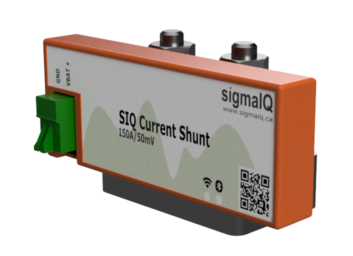
What is a Current Shunt
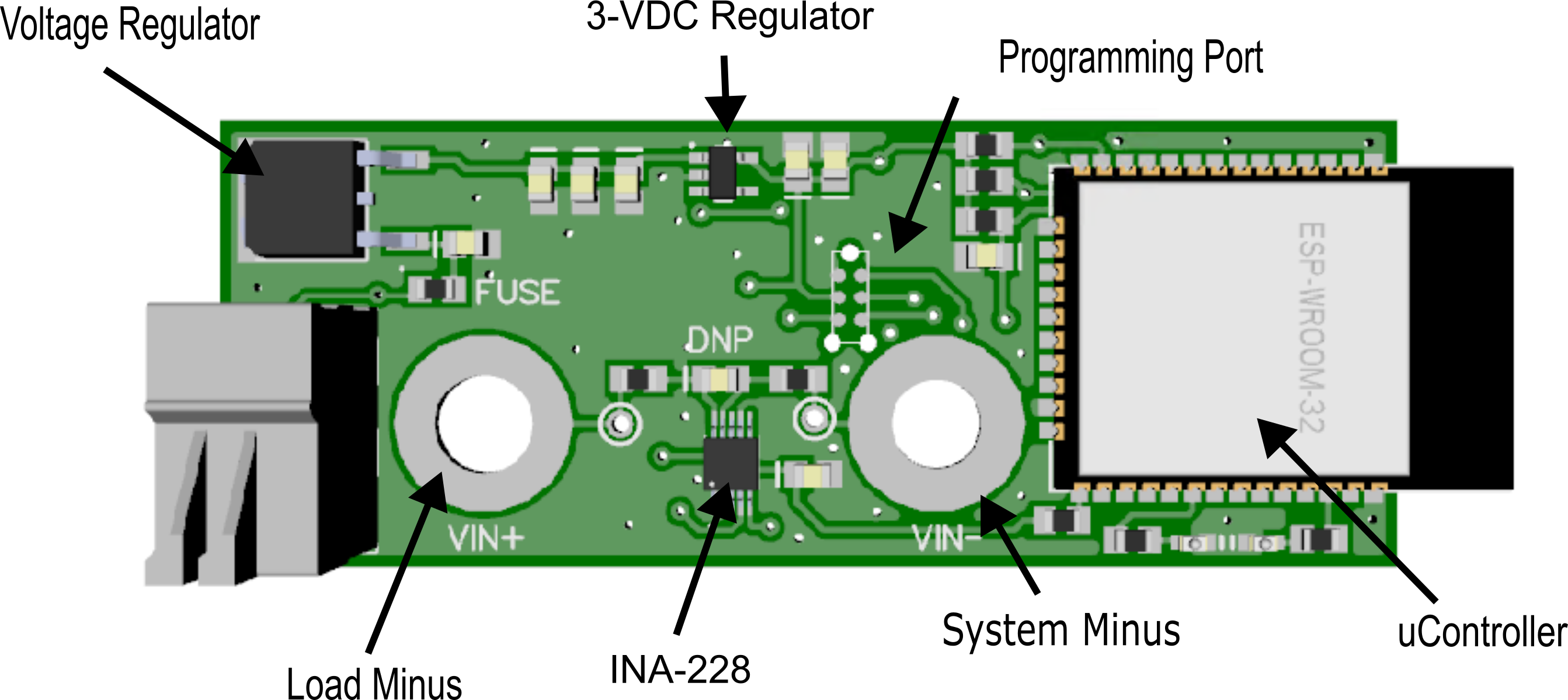
A current shunt is simply a device to measure current flowing in a circuit. A basic shunt can be made of a variety of materials such as a copper bar, a piece of wire or even a standard resistor. One thing all shunts have in common is they are all very low resistance. Electrically the shunt looks like a dead short, but as you are likely aware, any piece of wire, or copper bar has a small amount of resistance. This small amount of resistance works to our advantage when it comes to making a current measurement. Calculating the current in theory is quite simple, you just need to measure a very small voltage drop across the shunt terminals, and rearrange the V (voltage)=I(current)*R(resistance) formula to solve for I(current in amps). Simple in theory, little harder to do in practice. This is where the Texas Instruments INA228 and other equivalents comes into play. These chips do all the heavy lifting. The INA228 measures the voltage on each side of the shunt and calculates the voltage drop then along with some additional parameters that characterize the shunt it can calculate the current.
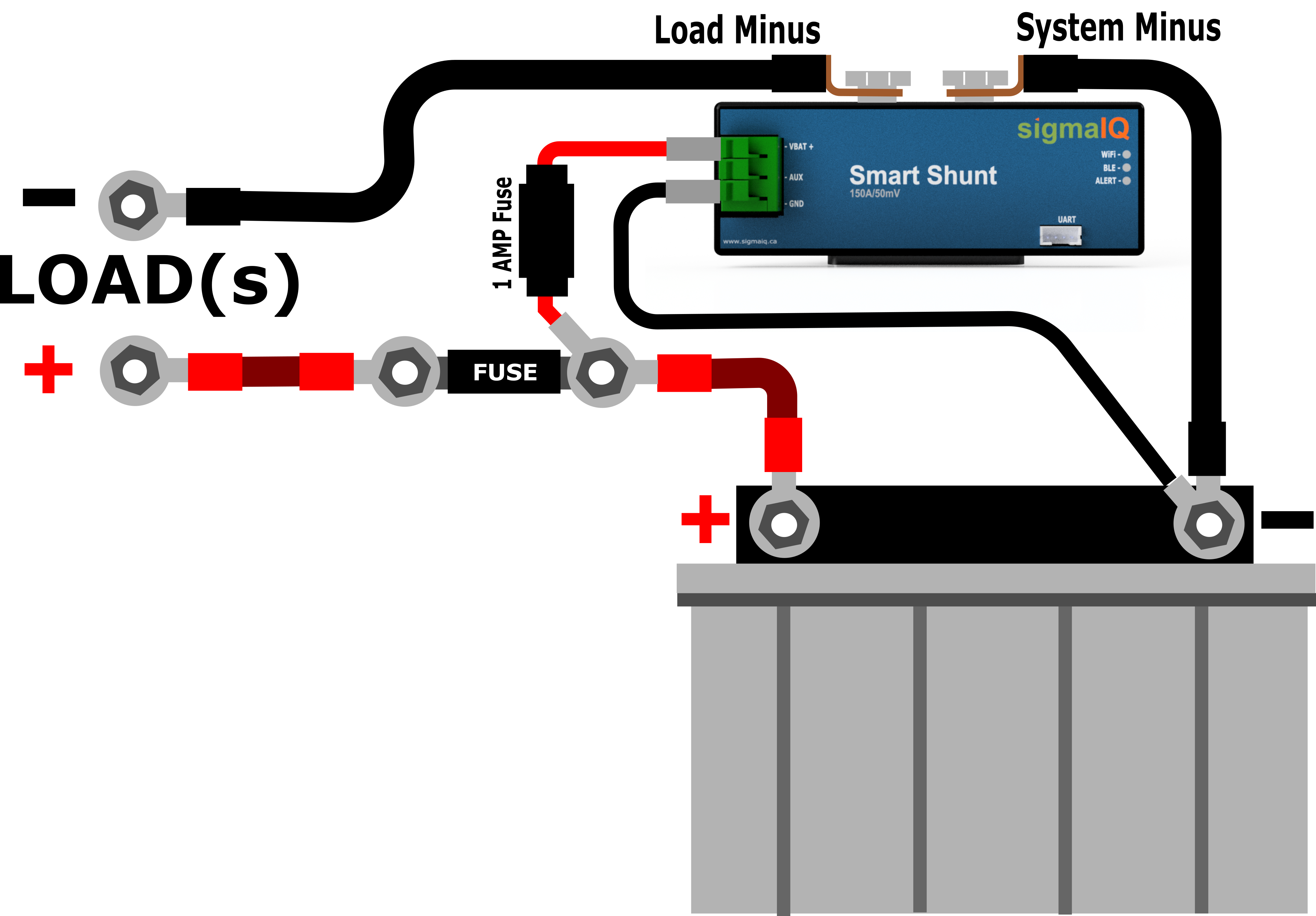
Current (Amps) = (VLoadMinus-VSystemMinus)/Shunt Resistance (ohms)
The INA228 provides additional information such as Consumed Energy (Joules), Charge (Coulombs), Power (Watts) as well as VBUS (voltage) and surprise surprise current (A).
Low Side Shunt
There are two typical deployments of current shunts, low side and high side. The reference design is a low side shunt only design. Using this shunt on the high side (positive leg) will result in the magic smoke being released, potential fire and definitely damage the equipment.
Data Sheets
- INA228 – 85-V, 20-bit, ultra-precise, I2C output current/voltage/power/energy/charge monitor
- ESP32-WROOM-32E – 32bit 2.4 GHz WiFi / Bluetooth LE module.
- ADP122AUJZ-3.3-R7 – Linear Voltage Regulator IC Positive Fixed 1 Output 600mA
- L7805CDT – Linear Voltage Regulator IC Positive Fixed 1 Output 1.2A
- 1-2834016-2 – 2 Position Wire to Board Terminal Block Horizontal
Parts List
Most of the parts in the system are not vendor critical, i.e. any of the capacitors and resistors can be sourced from anywhere. My recommendation is to stick with the Texas Instruments INA228 for the actual current measurement and the ESP-32-WROOM-32E for the microcontroller mainly because of the PCB footprint and firmware compatibility. Assuming the other parts are pin compatible and are within the specs of the components in the data sheet section provided above, you are likely good to go. The approximate cost of components is around $ 24.00 CDN.
The parts list and board placement drawing can be found here. This is an interactive html file that can assist with placing parts, as the component designators are turned off in the design. I would recommend downloading a local copy of the file to avoid issues with state.
Programming Cable

The programming cable I use is the Tag Connect TC2030-IDC-NL. This tag connect cable is connected to a FTDI Friend USB to UART adapter from Adafruit through a custom PCB that I developed for programming. The custom programming board contains a RESET and REBOOT switches for programming the ESP32 micro-controller.
In order for you to program the device you will need to be able to pull the RESET and/or BOOT pins to ground. To get the ESP32 into programming mode, hold the BOOT pin to ground and then hold the RESET pin low. If you did it right you should see a message on the console that the device is ready to receive a firmware update. I’ll admit this is a bit clumsy, but with the custom programming board uploading firmware is simple and easy.
Downloads
All the design files for the project can be found in my GitHub repository.
Conclusions
Assembly is easy, even with modest soldering skills. The capacitors and resistors are 0805 and are very manageable. The hardest component would be the INA228 but even that is doable. You could also have the PCB manufactures provide and place all the components if you don’t feel comfortable soldering. You will need to provide the manufacturer with a pick and place file. That functionality is built into Diptrace.
I have included a list of all the software you will need to turn this project into reality. Check out the repository. The PCB software that I currently use is Diptrace and while it is commercial software, the trial version will work for this project as the board size and pin counts are below the trial threshold.
Well thats it for this one. Cheers!